Scientific applications at MAXPEEM grow directly out of what the microscope can actually do. Its measurement modes naturally set the scope of the scientific questions that can be addressed. For that reason, the most intuitive way to explore MAXPEEM’s reach is to begin from the techniques themselves: how electrons are generated, how they are imaged, and what kinds of contrast they reveal. Once these operational modes are clear, their scientific uses unfold almost automatically.
MAXPEEM hosts an aberration-corrected photoemission and low-energy electron microscope (AC-SPELEEM). As the name suggests, it enables imaging of solid surfaces using two types of signal electrons: either photoelectrons emitted by X-ray/UV illumination or reflected electrons generated by an electron gun. By adjusting the lens settings, the microscope can project three different optical planes—real-space imaging, diffraction, and energy-dispersive planes on the screen. With additional photon mode selections, photoelectron detection in these three planes supports a wide range of operation modes:
- core-level XPEEM,
- secondary PEEM,
- XAS-PEEM,
- XMCD-PEEM,
- XMLD/XNLD-PEEM,
- micro-XPS, and
- photoelectron diffraction (micro-ARPES).
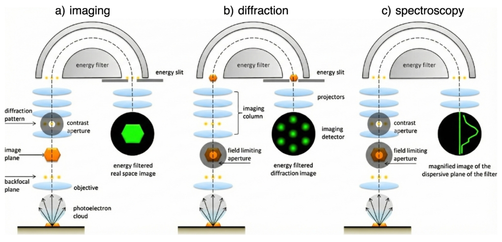
Fig. 1. Simplified schematic diagrams of three optical configurations in AC-SPELEEM: (a) real-space imaging, (b) diffraction plane, and (c) energy-dispersive plane. Adapted from T. O. Menteş and A. Locatelli, J. Electron Spectrosc. Relat. Phenom. 185, 323–329 (2012).
Similarly, using reflected electrons, the microscope provides complementary modes:
- MEM
- bright-field LEEM,
- LEED, and
- dark-field LEEM.
The following sections will describe these operation modes and their applications in more detail.
1) core-level XPEEM
In the core-level XPEEM mode, shown in Fig. 1a, the energy filter (a hemispherical energy analyser) transmits only those photoelectrons with a constant kinetic energy (the pass energy) within a narrow energy window defined by a narrow energy slit. The smaller the slit, the narrower the energy window. By varying the potential applied to the sample, known as the start voltage, photoelectrons with higher kinetic energies are retarded precisely to match the pass energy. Consequently, by scanning the start voltage in small steps, PEEM effectively probes the binding energies of photoelectrons, in accordance with the canonical photoemission equation,
Ek = hν − W − EB,
where Ek, hν, W and EB represent the photoelectron kinetic energy, the photon energy from the beamline, the effective work function of the microscope, and the binding energy of the core-level orbit, respectively. The resulting XPEEM images thus reflect the spatial distribution of selected core-level photoelectrons across the sample surface.
This capability allows core-level XPEEM not only to map elemental distributions, but also to distinguish between different chemical states of the same element. Such chemical sensitivity is exemplified in the case of GaAs: When a GaAs wafer is heated above its congruent temperature, As atoms evaporate more readily than Ga. The excess Ga atoms remaining on the surface form micron-sized droplets. Core-level XPEEM images can clearly reveal such GaAs surfaces containing two distinct Ga species—those bound within the substrate and those aggregated in droplets—when the binding energies of Ga3d are appropriately selected, as illustrated in Fig. 2.
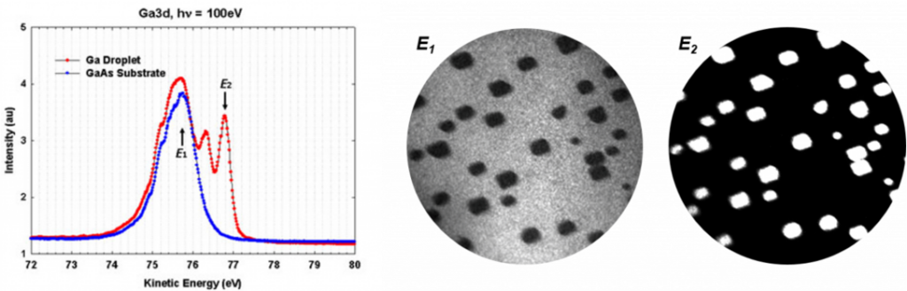
Fig. 2: (left) Micro-XPS spectra of Ga3d from a clean GaAs substrate and from a GaAs substrate with Ga droplets. (right) Core-level XPEEM images acquired at E1 and E2, corresponding to the Ga3d binding energies of the substrate compound and the metallic Ga droplets, respectively. The graph is adapted from unpublished data.
2) Secondary PEEM
Secondary PEEM, also referred to as threshold PEEM, operates at very low kinetic energies (low start voltages). In this mode, the imaging electrons are those with just enough energy to overcome the surface work function. Consequently, regions with lower work function appear brighter due to a stronger secondary photoelectron yield. For example, in the image below obtained from lithographically patterned gold bars on a Si wafer, the gold bars appear darker than the surrounding Si surface because gold has a higher work function. The illumination was provided by a mercury discharge lamp emitting 5 eV UV light. Secondary PEEM images taken with a mercury lamp generally provide better spatial resolution, since the energy spread of the photoelectrons is much narrower than that produced by higher-energy X-ray excitation. A narrower energy spread leads to reduced chromatic aberration, which would otherwise unavoidably blur the image.
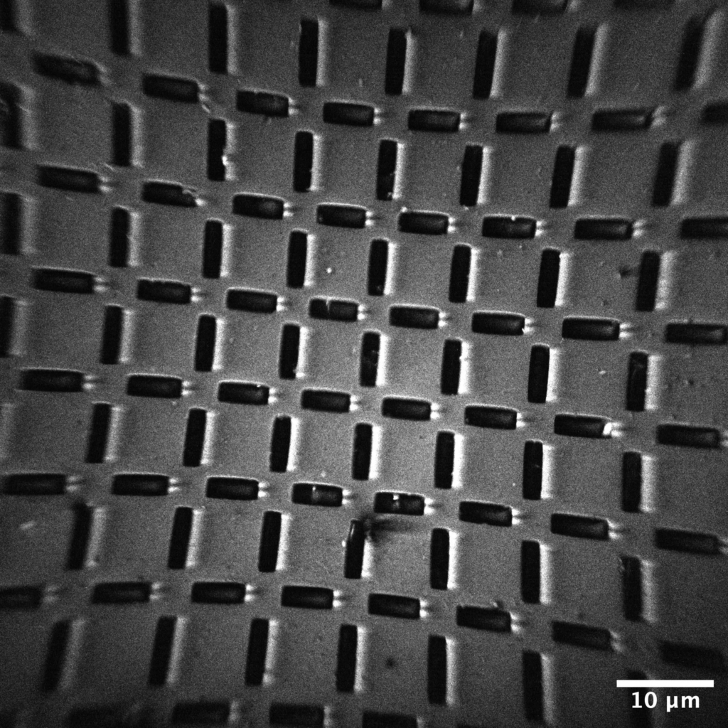
Fig. 3. Secondary PEEM (UV-PEEM) image acquired under 5 eV UV illumination. The graph is adapted from unpublished data.
3) XAS-PEEM
In conventional X-ray absorption spectroscopy (XAS), all photoelectrons are detected by measuring the drain current of the sample with an electrical current meter, a method known as total electron yield (TEY). The majority of the signal in TEY originates from secondary photoelectrons. At MAXPEEM, this principle can be extended by recording secondary PEEM images while scanning the photon energy across an absorption edge, thereby obtaining spatially resolved XAS spectra in the partial electron yield (PEY) mode.
As an example, we examined a rock sample from the Central Lapland Greenstone Belt in Finland, formed approximately two billion years ago. XAS spectra enable analysis of the chemical states of Fe and Cr oxides in the sample. For instance, a higher Fe3+/Fe2+ ratio typically indicates formation under more oxidizing conditions. Quantitative evaluation of this ratio generally requires comparison with standard Fe3+ and Fe2+ reference samples.
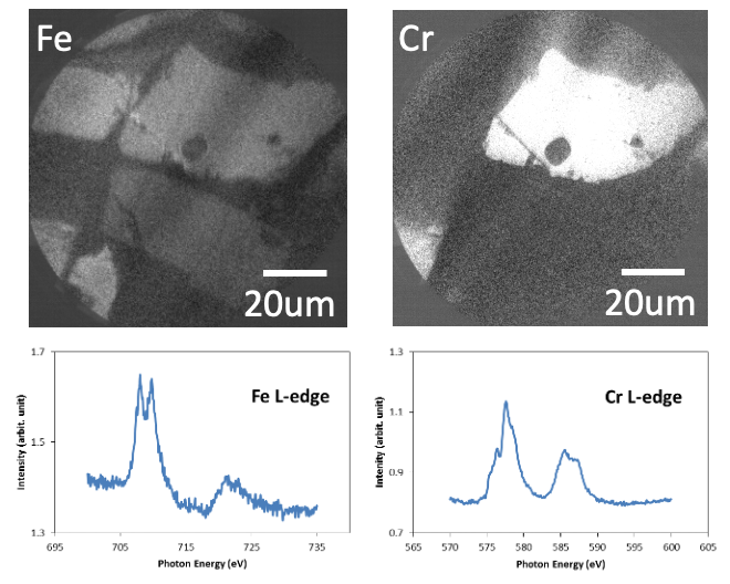
Fig. 4. a) XAS-PEEM image taken at Fe L-edge, E= 708 eV; b) select area XAS spectrum taken from an Fe-rich grain; c) XAS-PEEM image taken at Cr L-edge, E = 577eV; d) select area XAS spectrum taken from the grain at upper right of c). Adapted from unpublished data.
4) XMCD-PEEM
Checking the polarization dependence of XAS-PEEM naturally leads to the development of XMCD-PEEM and XMLD/XNLD-PEEM techniques. For example, the L-edge XAS of Fe, Co, and Ni originates from the excitation of electrons from the 2p core levels into unoccupied 3d states. In ferromagnetic materials, the transition probabilities of these photoelectrons depend on the helicity of the X-rays, i.e., left- and right-circularly polarized light. Magnetic contrast is obtained by differentiating two images acquired with opposite helicities, defined as
(Iσ+ − Iσ−) /(Iσ+ + Iσ−)
This contrast, IXMCD, is proportional to PSP · m, where P is the degree of polarization, SP is the spin angular momentum of the light, and m is the local magnetic moment. At MAXPEEM, the X-rays are incident normal to the sample surface; therefore, IXMCD ∝ PSP · m implies that only the out-of-plane magnetization component is detectable, but with 100% sensitivity. Please note that at MAXPEEM, the first-harmonic radiation provides 100% polarization only up to 300 eV. At higher photon energies, elliptically polarized light is generated, with a degree of polarization of 80–90%, depending on the undulator settings.
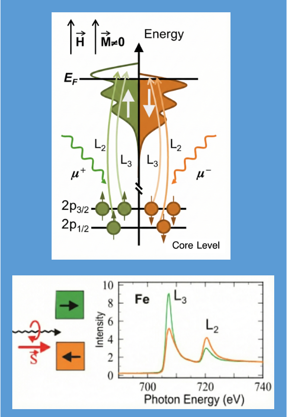
Fig. 5. (upper) Schematic two-step picture of XMCD for a single electron in the resonant excitation process of a magnetic material, adapted from G. van der Laan and A. I. Figueroa, Coordination Chemistry Reviews 277–278, 95 (2014). (lower) Illustration of the magnitude of magnetic dichroism effects, adapted from SSRL.
As an example, we consider a Pt/Co multilayer with perpendicular magnetic anisotropy (PMA). As shown in Fig. 6, XMCD-PEEM reveals characteristic labyrinth domains in the Pt/Co multilayer with very high contrast and spatial resolution.
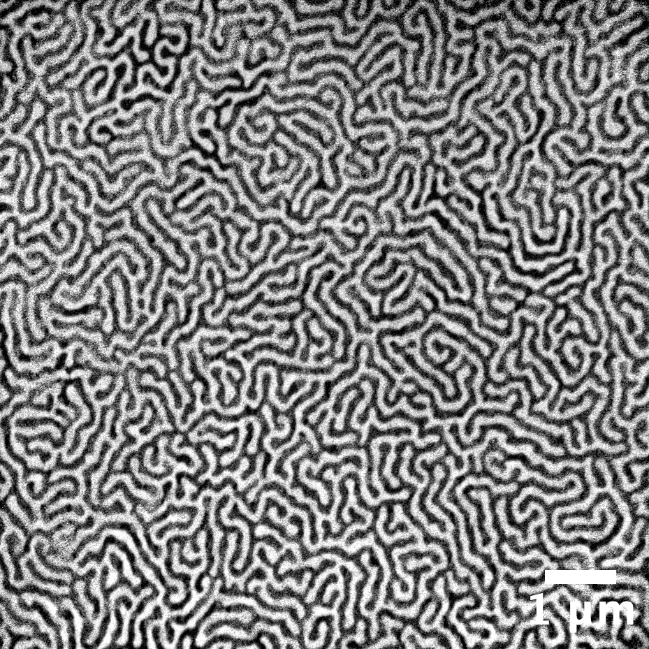
Fig. 6. XMCD-PEEM image of a Co/Pt multilayer thin film grown on Si. The black and white contrasts indicate magnetic domains with magnetization oriented either upward or downward relative to the film plane. Adapted from unpublished data.
5) XMLD/XNLD-PEEM
X-ray magnetic linear dichroism (XMLD) and X-ray natural linear dichroism (XNLD) both arise from the dependence of X-ray absorption on the polarization direction of linearly polarized light. In XMLD, the effect originates from magnetically induced anisotropy in the unoccupied electronic states: the exchange field and spin–orbit coupling cause the absorption cross section to differ for linear polarizations parallel and perpendicular to the local magnetization axis. In contrast, XNLD arises from purely structural anisotropy of the local environment, i.e. the non-cubic crystal field around atoms, independent of magnetism. Thus, XMLD and XNLD share the same basic principle—linear polarization probes anisotropy in unoccupied states—but differ in origin: XMLD reflects magnetic ordering, whereas XNLD reflects crystal-field symmetry. For ferromagnetic materials, the XMLD contrast can be expressed as
IXMLD ∝ P|m · E|2,
where P is the degree of linear polarization, m is the local magnetization, and E is the electric field vector of the linearly polarized light. For antiferromagnetic materials (in the collinear case), m should be replaced by the Néel vector, N, defined as N = mA − mB, where mA and mB are the magnetic moments of the two sublattices. In contrast, for XNLD from a non-magnetic sample, m should be replaced by a local structural anisotropy vector, giving
IXNLD ∝ P|n · E|2,
where n can represent a ferroelectric polarization vector, a local crystal-field axis, or another structural anisotropy direction.
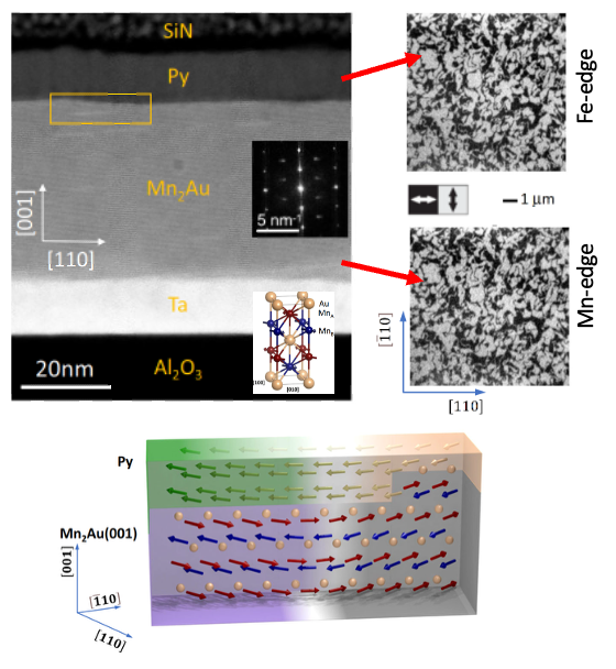
Fig. 7. (a) Cross-section HAADF-STEM image of the Mn2Au/Py stack along the [-110] direction. Insets show a local Fourier transform of the Mn2Au(001) region and the Mn2Au crystal structure with magnetic moments along the easy [-110] axis. (b) XMLD-PEEM images of AFM domains in Mn2Au (top) and corresponding FM domains in Py (bottom); dark contrast indicates N and MF right–left, bright contrast up–down. (c) Schematic of the bilayer showing two 90° domains and illustrating how the AFM domain pattern is imprinted into the FM through the Au-terminated interface. This graph is adapted from S. P. Bommanaboyena, D. Backes, et al., Nat. Commun. 12, 6539 (2021).
Another strength of MAXPEEM lies in its ability to combine XMCD-PEEM and XMLD-PEEM for nanoscale studies of altermagnetism, enabled by its unique normal-incidence geometry. Altermagnets, such as MnTe, break time-reversal symmetry like ferromagnets yet exhibit zero net magnetization, as in antiferromagnets. This makes them highly promising for spintronics, but also very challenging to characterize. Spatially averaged probes often miss the subtle spin configurations that define the altermagnetic order.
Using XMCD-PEEM and XMLD-PEEM, we can directly image magnetic domains at the nanoscale. XMCD is sensitive to spin polarization and reports time-reversal symmetry breaking, while XMLD reveals the orientation of the altermagnetic order parameter, L = M1 − M2, even in the absence of net magnetization. Together, the two techniques are complementary and enable domain-resolved mapping of altermagnetic textures directly in real space.
A recent demonstration of this approach was reported for MnTe in Nature , where XMCD- and XMLD-PEEM were used to resolve nanoscale altermagnetic domains and visualize their symmetry-breaking character. Fig. 8 from that study illustrates how the two contrasts provide complementary information; the detailed explanation is given in the caption.
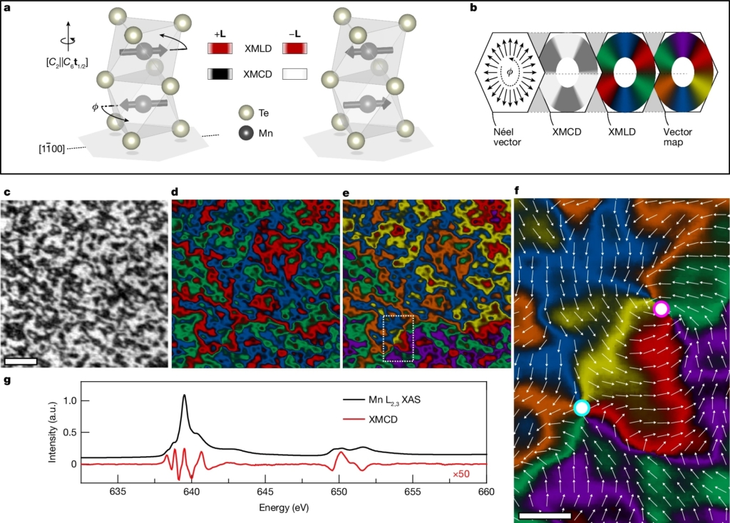
Fig. 8. XMCD/XMLD-PEEM mapping of altermagnetic MnTe. a, Unit cell of αMnTe with Mn spins collinear to the in-plane easy axis. Unit cells with opposite L yield identical XMLD but opposite XMCD due to time-reversal–symmetry breaking.b, Vector-mapping scheme: XMCD modulates the three-colour XMLD wheel to produce a six-colour map of the in-plane L-vector orientation (coloured segments mark the easy-axis directions).c–e, XMCD-PEEM (c), XMLD-PEEM (d) and resulting six-colour L-vector map (e) for a 25-μm² region of unpatterned MnTe (scale bar, 1 μm).f, Zoom of e showing a vortex–antivortex pair (core positions highlighted; scale bar, 250 nm).g, XAS (black) and XMCD (red, ×50) across the Mn L₂,₃ edges (a.u.). Adapted from O. J. Amin et al., Nature 636, 348–353 (2024).
6) micro-XPS
As shown in Fig. 1c, by adjusting the last two projection lenses (P2 and P3) in the AC-SPELEEM, the dispersive plane of the hemispherical analyzer can be projected onto the final detector. This dispersive plane also corresponds to the location of the energy slit when energy filtering is applied, i.e., in imaging mode (Fig. 1a) and diffraction mode (Fig. 1b). For the Elmitec R200 analyzer used at MAXPEEM, the full dispersive plane spans about 6 eV on the detector. In micro-XPS measurements, a select-area aperture is placed in the image plane to define the measurement area. A contrast aperture is also employed to improve the energy resolution, which can reach up to 60 meV. Micro-XPS is typically used as a complementary technique to core-level XPEEM, as illustrated in Fig. 2.
As an additional example, we consider KTiPO4, a ferroelectric material that can be poled into distinct polarization domains. Within these domains, K+ ions shift along the electric field direction, resulting in surface accumulation in the positively polarized regions. This is confirmed by core-level XPEEM imaging of the K3p signal. When the select-area aperture is positioned over two different domains, micro-XPS spectra reveal variations in the K3p peak intensity, again confirming enhanced K concentration in the positively polarized domains.
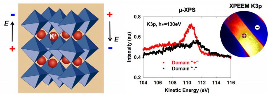
Fig. 9. Micro-XPS characterization of ferroelectric domains in KTiPO4. (left) Crystal structure of KTiPO4 showing the displacement of K+ ions along the polarization direction. (right) Micro-XPS spectra of the K3p core level acquired with hν = 130 eV from two oppositely poled domains. The K3p peak intensity is higher in the positively polarized domain (“+”), indicating surface enrichment of K+ ions. The inset shows the select-area aperture positioned on two domains in the corresponding core-level XPEEM image. Adapted from unpublished data.
7) photoelectron diffraction (micro-ARPES)
The operation mode of photoelectron diffraction is illustrated in Fig. 1(b). In this configuration, the diffraction plane of the hemispherical analyzer is projected onto the final detector by a specific lens setting. With the use of a select-area aperture, regions as small as ~1 µm on the sample surface can be probed.
In the micro-ARPES mode, the photon energy and the start voltage are tuned so that valence-band photoelectrons are recorded with fine energy steps within the energy window defined by the analyzer’s slit. Unlike conventional ARPES instruments, which typically measure energy–momentum dispersions along selected k-cuts, micro-ARPES at MAXPEEM acquires the band structure in an equal-energy contour mapping mode: the entire kx–ky momentum space is captured simultaneously at a constant binding energy. This is conceptually similar to the operation of modern momentum microscopes (also referred to as k-PEEM).
Such a mode is particularly advantageous for identifying Fermi surface topology, mapping anisotropic band dispersions, and analyzing photoelectron diffraction features from specific micro-domains. Combined with the spatial selectivity of the aperture, micro-ARPES enables domain-specific band structure measurements, which are not accessible with standard ARPES setups. This advantage is clearly demonstrated with the example of Ge-interclated graphene on SiC.
In Fig. 10, an XPEEM image taken with Si2p core-level photoelectrons reveals two coexisting regions with different amounts of Ge atoms intercalated at the interface. By placing the select-area aperture on each regions, one can directly measure their local band structures that both present characteristic Dirac cones of graphene but with distinct doping types. For the p-type domain (left), the Dirac point is located at 0.13 eV above the Fermi level, consistent with hole doping. In contrast, for the n-type domain (right), the Dirac point shifts downward to 0.23 eV below the Fermi level, indicating electron doping.
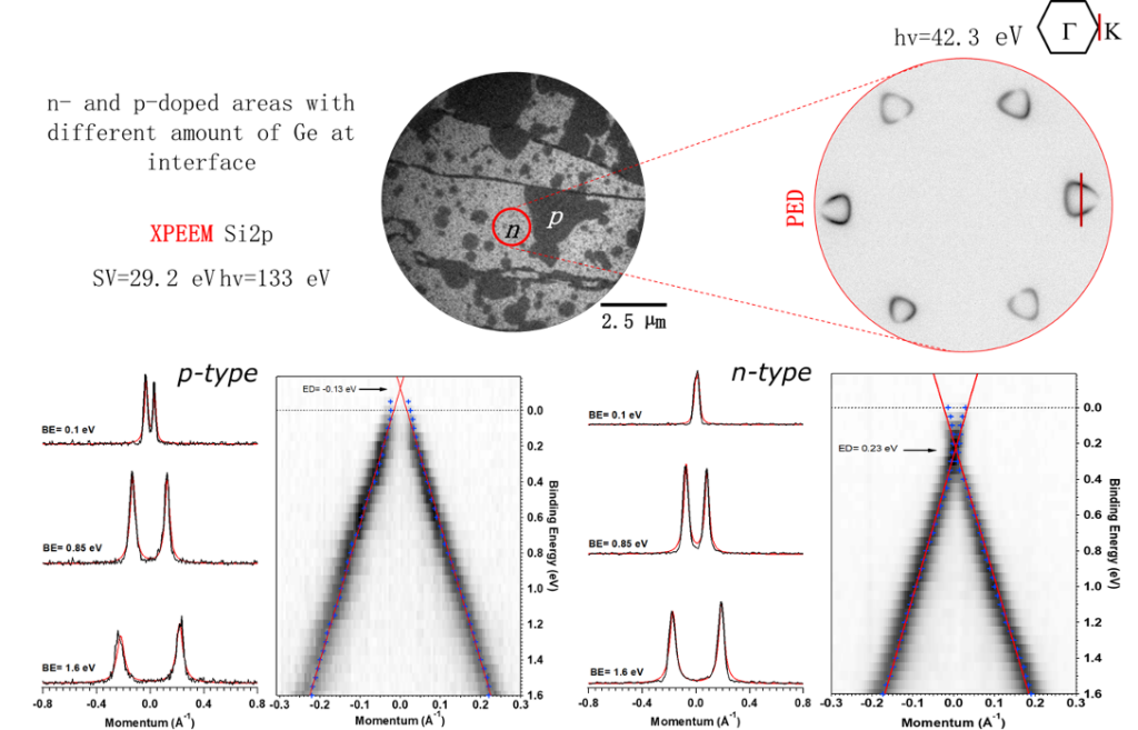
Fig. 10. Micro-ARPES study of Ge-intercalated graphene on SiC. (upper) Core-level XPEEM image at the Si2p orbit showing two regions with different Ge intercalation. The inset shows a single micro-ARPES raw image from n-type region. (lower left/right) Local band structures reveal characteristic graphene Dirac cones with p-type and $n$-type doping, respectively. Momentum distribution curves (MDCs) confirm the different Fermi surface sizes of the two domains. This graph is adapted from Y. R. Niu, et al., J. Synchrotron Rad. 30, 468–478 (2023).
8) MEM
The electron gun in the microscope provides a valuable complementary probe, particularly for ordered surfaces and interfaces. The landing energy of the electron beam is controlled by the start voltage. When the landing energy is negative or close to zero, the electron reflectivity approaches 100%, so that the sample acts like an electron mirror. This operation mode is referred to as mirror electron microscopy (MEM). At higher landing energies, the electrons begin to interact with the sample: the reflectivity decreases but remains at a reasonable level, especially for many ordered surfaces. While LEEM is often used as a broad term that also includes MEM, in this work we adopt the narrower definition and use LEEM only to refer to the regime above MEM.
In MEM, as shown in Fig. 11(a), the electrons are highly sensitive to the surface electric field of the sample. Even small variations in surface height, work function, or electrical polarization can deflect the electron trajectories and thus produce strong contrast in the final image. To a certain accuracy, the transition from MEM to LEEM, e.g. the energy at which the reflectivity drops to 50%, or so called the inflection point can be used to quantified the work function of sample surface. In this sense, the area with higher work function enter the LEEM region at higher start voltage.
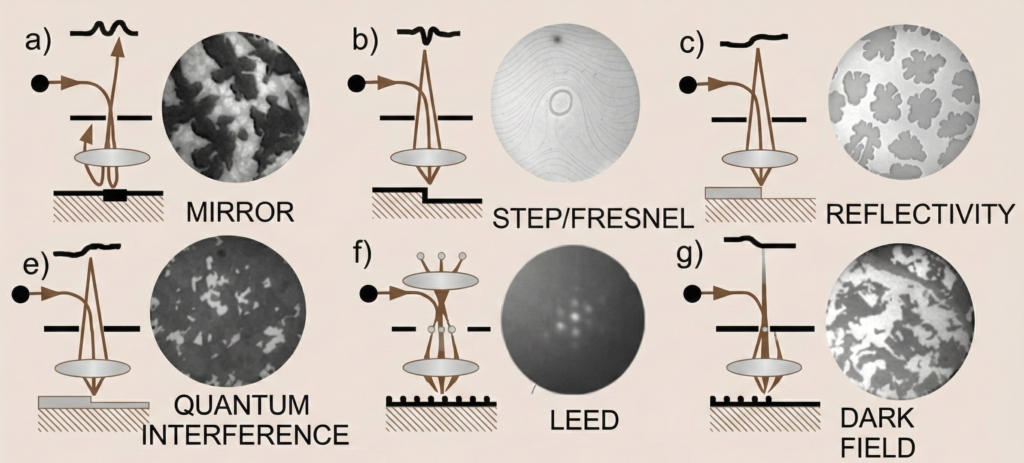
Fig. 11. Various operation modes/imaging mechanisms with the electron beam. The graph is adapted from https://surfmoss.iqfr.csic.es/en/16-equipment/31-introduction-to-leem
9) bright-field LEEM
The most common imaging mode using the electron beam from the gun is bright-field LEEM, where the specularly reflected (00) beam is selected by the contrast aperture. Bright-field LEEM can provide several contrast mechanisms, depending on the sample and the microscope settings. For example, as shown in Fig. 11(b), a slight defocus causes destructive interference between reflected beams from adjacent terraces, producing a dark line contrast at the steps. In this sense, bright-field LEEM can be regarded as an imaging technique with single-atomic-layer sensitivity along the surface normal.
The reflectivity of low-energy electrons is highly sensitive to surface structures and even to buried interfaces, and in many cases it is strongly energy dependent (Fig.11(c)). The detailed variation of reflectivity with electron energy—so-called LEEM IV curves—serves as a characteristic fingerprint of different materials, phases, and structures. At selected energies, where the contrast is maximized, bright-field LEEM can be applied to monitor thin-film growth, phase transitions, and other dynamic surface processes in real time at video rates.
A particularly important contrast mechanism responsible for oscillations in LEEM IV curves is quantum size interference, where electron waves reflected from the film surface and from the interface interfere constructively or destructively depending on their energy (Fig. 11(d)). One of the most widely used applications of this effect is the thickness determination of graphene films: the number of minima in the LEEM IV curve directly corresponds to the number of graphene layers, as shown in Fig. 12.
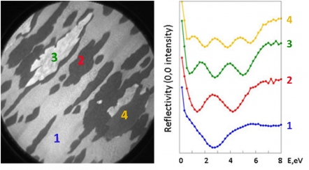
Fig. 12. (a) Bright-field LEEM image showing terrace contrast, with the local thicknesses further determined from (b) LEEM IV curves. The graph is adapted from C. Virojanadara et al. J. Phys. D: Appl. Phys. 43 374010 (2010).
10) micro-LEED
Projecting the diffraction plane of the microscope under electron illumination produces low-energy electron diffraction (LEED) patterns of the surface structure on the detector. In a LEEM instrument, the illuminated area can be restricted with an aperture, a mode known as select-area LEED or micro-LEED (Fig. 11(e)). This allows diffraction to be collected from specific sample regions for detailed structural analysis. Because the illuminated region is reduced, the diffraction pattern is less affected by lateral inhomogeneities, and the resulting micro-LEED spots are typically sharper and better defined than in conventional LEED.
Here we use this sample to illustrate how Sn intercalation converts the buffer-layer graphene on SiC into quasi-free-standing graphene. Comparing the non-intercalated region (Fig. 13b) with the intercalated region (Fig. 13c), the graphene’s diffraction spots become much more pronounced after Sn intercalation. Complementary XPEEM and micro-XPS measurements (Fig. 13d–h), together with micro-ARPES (not shown), further confirm the presence of Sn at the interface.
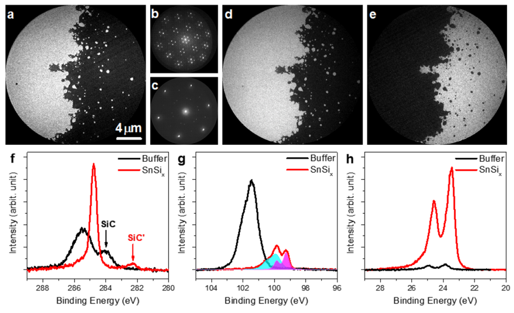
Fig. 13. (a) bright-field LEEM image and (b,c) μ-LEED patterns recorded at room temperature from the buffer layer region and the SnSix-intercalated region after annealing to 1050 °C. The distinct diffraction patterns confirm the structural change induced by Sn intercalation. Complementary XPEEM and μ-XPS measurements (d–h) further verify the presence of Sn at the interface. The graph is reprinted from Y. R. Niu et al., Ultramicroscopy, 183, 49-54 (2017), with permission from Elsevier.
Another key advantage of micro-LEED in LEEM is that the diffraction spot positions remain fixed when the landing energy of the electron beam is varied. This results from the fact that the electrostatic field between the sample and the objective lens compresses the diffracted beams in an energy-dependent way, exactly compensating the intrinsic energy dependence of the diffraction angles. As a result, the analysis of LEED-IV curves becomes much more straightforward.
11) dark-field LEEM
When a higher-order diffracted spot, rather than the specular (00) beam, is selected in LEED mode using the contrast aperture, the microscope can be switched back to imaging mode to form a LEEM image solely from this diffracted beam. This operation mode is known as dark-field LEEM (Fig.11(f)). In this mode, regions of the sample that satisfy the selected diffraction condition are highlighted, providing strong sensitivity to crystallographic orientation, structural domains, and defects. For instance, on surfaces with rotationally equivalent domains, different diffraction spots can be selected to image individual domains, yielding domain-resolved maps with nanoscale spatial resolution. Dark-field LEEM is therefore widely applied to investigate structural domains, surface reconstructions, stacking faults, and epitaxial relationships in thin films and two-dimensional materials.
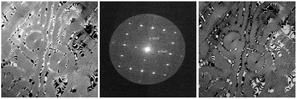
Fig. 14. Dark-field LEEM images of two Si(001) surface reconstructions: (left) (2×1) and (right) (1×2), obtained by selecting the corresponding diffracted beams. The central panel shows the LEED pattern of the Si surface with the diffraction spots labeled. Adapted from unpublished data.
Further reading
- https://link.springer.com/book/10.1007/978-1-4939-0935-3
- https://link.springer.com/chapter/10.1007/978-3-030-46906-1_13
- https://surfmoss.iqfr.csic.es/en/16-equipment/31-introduction-to-leem
- https://www.tandfonline.com/doi/full/10.1080/23746149.2025.2549757
- https://www-ssrl.slac.stanford.edu/stohr/xmcd.htm