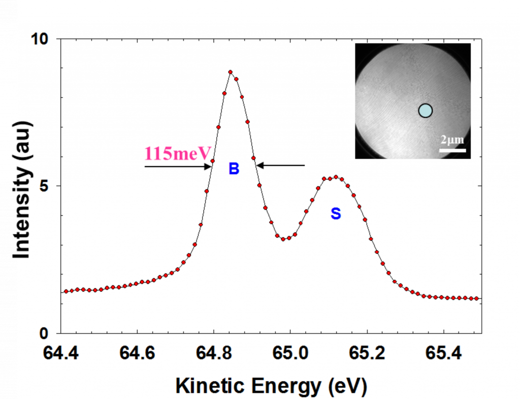
Energy resolution
The energy resolution in the various acquisition modes is: better than 0.2 eV in XPEEM; 0.15 eV in μ-XPS and 0.15 eV in μ-ARPES.
Spatial resolution
The spatial resolution is calculated for the various acquisition techniques in correspondence to the respective AC Mirror status (OFF, ON).
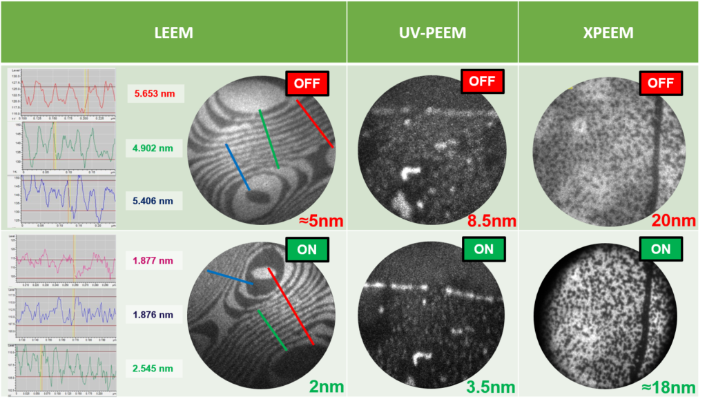
(Left) LEEM: Si(001), Dark field image of (1X2) and (2X1) terraces. FoV=750 nm, STV=4.3 eV. (Centre) UV-PEEM: Graphene/Au/SiC(0001), n- and p-doped areas with different amount of Au at the interface. FoV=750 nm, STV=0 eV. (Right) XPEEM: Graphene/Ge/SiC(0001), n- and p-doped areas with different amount of Ge at the interface. FoV=2500 nm, STV=3 eV, hv=133 eV.
Resolution in k space
The Fermi surface mapping in the full cone is possible in µ-ARPES. The first Brillouin zone is acquired from selected areas (0.89 µm2) on monolayer (blue circle on the LEEM image) and bilayer (green circle on the LEEM image) graphene allowing the extraction of the line cuts of the Dirac cones and providing a wavevector resolution better than 0.15 Å⁻¹.
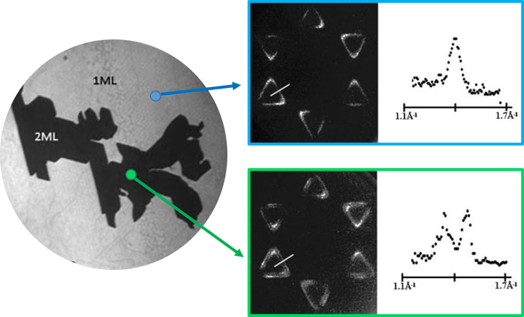
(Left) LEEM: Gr/Si(001) 1ML graphene with 2ML islands. FoV= 20 µm, STV= 4.6 eV. The dimension of the circles on the LEEM image corresponds to 0.89 µm2. (Right) Photoelectron diffraction pattern taken at an electron binding energy of 2.5 eV below the Fermi level from the selected area on 1ML (blue circle on the LEEM image) and on 2ML (green circle on the LEEM image) graphene. The high energy resolution 2D maps (energy resolution of 0.15 eV) are acquired using a photon energy of hv= 35 eV. The respective line cuts of the Dirac cones are shown on the right. Two π-bands are clearly seen from the 2ML island.
A.A. Zakharov et al. J. Electron Spectros. Relat. Phenomena 185, 10 (2012)