By growing superlattices consisting of ferroelectric and non-ferroelectric transition metal oxides and releasing them from their underlying substrates, researchers explore polarization patterns in curved geometries.
Complex transition-metal oxides are often sensitive to strain and may display very different properties if their lattice is compressed or extended. This is especially true of ferroelectric materials, such as lead titanate, which have a switchable spontaneous electrical polarization that is strongly coupled to the distortion of the lattice.
This sensitivity to strain is exploited in “strain engineering,” which allows material properties to be enhanced, or even wholly new properties to be induced, by manipulating the lattice. Conventionally, strain is induced by growing a thin film or a multilayer on a monocrystalline substrate in a way that the lattice of the film is squeezed or stretched to match that of the substrate. However, once the material has been planted on the substrate, it becomes very difficult to deform or manipulate it further, which strongly limits its electromechanical response. The dominant effect of the substrate can also hinder the emergence of potentially interesting new behaviors that may arise from the elastic interactions between the individual components in multilayer structures.
Therefore, scientists from University College London, Imperial College London, the Czech Academy of Sciences, Delft University of Technology, University of Geneva, University of Limerick, SuperSTEM Laboratory, ESRF and MAX IV decided to grow a heterostructure that combines a superlattice consisting of alternating layers of ferroelectric lead titanate and paraelectric strontium titanate, with a strontium ruthenate bottom electrode, and then remove it from its substrate. This then allowed the scientists to examine how the electrostatic and elastic interactions between the individual layers affect the structure and polarization patterns in the free-standing superlattice.
Removal of the mechanical constraint from the substrate, which would otherwise dominate over the electrostatic forces, created a more level playing field in the competition between electrostatics and elasticity.
“Because of its composition and layered structure, the electrostatic boundary conditions in the superlattice lead to a depolarizing effect that favors the polarization in the lead titanate to rotate into the plane of superlattice film. This, in turn, causes the lattice parameter of the superlattice layer to elongate along the polarization direction. At the same time, the strontium ruthenate layer below it, which naturally has a smaller lattice parameter, exerts a compressive stress on the superlattice from the bottom. These two competing forces cause the whole heterostructure to bend and curl up into a tube,” explained Pavlo Zubko, Professor of Physics at London Centre for Nanotechnology at UCL.
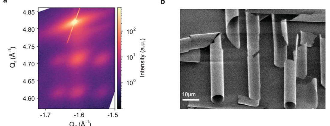
Using a combination of different experimental techniques, including synchrotron-based scanning X-ray diffraction imaging, Raman scattering, piezoresponse force microscopy, and scanning transmission electron microscopy, the team then studied the complex arrangement of nanoscale domains—regions with the same orientation of the polarization—in the curved superlattice tubes.
To map out the structure and domain arrangements, the scientists performed local synchrotron-based X-ray diffraction measurements. Because of the small size and the curved geometry of the tubes, this required the very fine beam provided by MAX IV’s NanoMAX beamline.
“The tubes are about 8 microns in diameter, so we needed a probe which is very small, and NanoMAX allowed us to focus the beam to less than 100nm in size in our experiment. We could probe the local crystallography of these structures and, of course, it allowed us to see what happens throughout the depth of the very thin film that is being probed. We learned that the polarization structure was more complicated than we originally expected,” said Zubko.
Ferroelectric materials are important in a wide range of applications that rely on their electromechanical responses such as sensors and actuators and are exploited in electronic applications as dielectrics in capacitors, memories and transistors. Although at present, their research is mainly fundamental, the scientists are hoping that understanding the behavior of nanoscale domains in curved structures such as these will contribute to the efforts in the development of ferroelectrics-based flexible electronics and more compact devices based on 3-dimensional architectures.
“The cool thing is, once you can remove a film from a substrate, you can put it on anything you want. One of the difficulties with most ferroelectrics was always their compatibility with silicon and silicon technologies. It’s very hard to grow them on silicon well without affecting the properties of the silicon substrate, and so transferring the films from a different substrate opens a lot of possibilities for integrating them with technology that is already out there,” said Zubko.