Scientists examined whether honeycomb boron can function as a structural analogue 2D material to graphene. Employing core-level X-ray spectroscopies, scanning tunneling microscopy, and DFT calculations, they analyzed the structure and electronic properties of honeycomb boron after its reaction with aluminum. They found that although it resembles graphene in electronic structure to some extent, it fails to form a quasi-freestanding monolayer on aluminum. This lack of a freestanding state is a clear difference from the behavior of graphene or monolayer hexagonal boron nitride (h-BN) on lattice-mismatched metal surfaces.
Borophene is a collective name for quasi-freestanding 2D boron sheets or crystalline atomic monolayers of boron. Typically, such sheets have to contain periodic B vacancies to maintain structural stability, and these vacancies may appear in a great variety of different motifs. This makes borophene a highly polymorphic material. An extra charge transfer to or from the borophene (e.g. via the supporting substrate) can modify the material’s motif and properties further, thus allowing scientists to create different borophene forms. This polymorphic nature sets borophene apart from graphene.
“One can imagine hundreds of different borophene sheets, with different shape, size and composition of the unit cell and different concentration of periodic B vacancies; some will be stable and some not. This is something you cannot do with graphene, which is just honeycomb, you cannot create anything else from carbon atoms in 2D,” said Dr. Alexei B. Preobrajenski, beamline scientist at MAX IV’s FlexPES beamline.
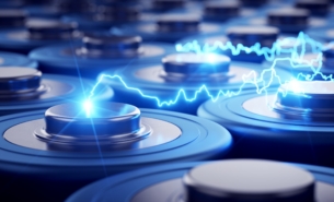
This polymorphism has raised new interest in 2D boron sheets as scientists discovered first stable borophene allotropes on Ag(111) [1]. Materials including borophene are promising for various technological applications ranging from batteries and supercapacitors to sensors and catalysis.
One way to grow 2D boron sheets experimentally is by placing boron on top of different metallic substrates at elevated temperatures, which allows to control the strength of interaction between the sheet and the substrate. This also allows for different degree of electron doping from the substrate, that is generating either a surplus or a deficiency in valence electrons within the material. Generally, this approach allows researchers to examine and to manipulate the conductivity of semiconductors. In the case of borophene, it can enable the formation of specific allotropes with desired structure and properties.
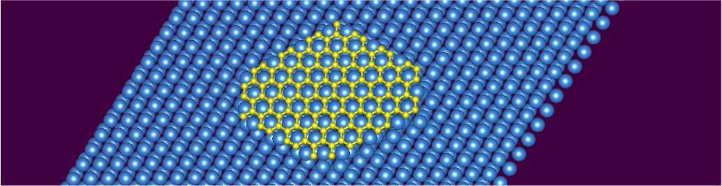
Dr. Preobrajenski and his colleagues from Hokkaido University, St. Petersburg State University, and MAX IV followed the recipe known from 2018 where scientists formed a single layer of honeycomb boron on top of aluminum [2] in order to study the structural and electronic properties of this sheet with x-ray spectroscopic techniques, Scanning Tunneling Microscopy, and Density Functional Theory calculations.
The experimental part of the project was carried out at MAX IV while the colleagues from Hokkaido University in Japan performed the theoretical calculations. Following high-resolution XPS spectroscopy, the scientists could reveal details of the boron sheet growth on Al(111) and observe the resulting charge transfer from the substrate, while x-ray absorption spectroscopy with angular resolution allowed them to access the unoccupied electronic structure of this material and probe in-plane (s*) and out-of-plane (p*) electronic sub-systems separately.
“If you have access to the tool which can separate these two electronic subsystems, you can also compare honeycomb boron with graphene and see how different the materials really are. This was the main motivation for us from the experimental point of view,” said Dr. Preobrajenski. “Honeycomb boron is an extreme case of borophene with a maximum possible concentration of B vacancies… This is a material which is electronically unstable. It cannot exist without any substantial electron doping. What aluminum substrate is doing here is two things. Firstly it is pumping just the right amount of electrons to make it stable and secondly it is almost lattice-matched to the honeycomb boron.”
If the resulting material was a structural analogue to graphene, then it would wiggle like a blanket and could corrugate on the aluminum substrate to accommodate the small mismatch. However, upon close examination using x-ray spectroscopies and DFT, the researchers found that the material was strongly bound and matched to the topmost metal layer, which in turn was mismatched relative to the underlying metal substrate forming a stoichiometric single-layer AlB2 [3]. This conclusion is in line with another recent report based on the ARPES technique [4]. In other words, honeycomb boron essentially matched the metallic substrate aluminum’s structure so closely that it could not be considered an independent, freestanding layered material.
“Our soft x-ray spectroscopic methods are particularly suitable in the research on different borophene allotropes, as they provide direct access to the chemistry and electronic structure of these intriguing materials, and allow to study their interactions with substrates and adsorbates. A large variety of growth processes and on-surface reactions can be followed and understood using high-resolution synchrotron-based XPS and XAS available at soft x-ray beamlines at MAX IV, especially in combination with STM and DFT calculations,” said Dr. Preobrajenski.
[1] Mannix A. J. et al., Science 2015, 350, 1513; Feng, B. et al., Nature Chem. 2016, 8, 563.
[2] Li W. et al., Sci. Bull. 2018, 63, 282.
[3] Preobrajenski A. et al., ACS Nano 2021, 15, 9, 15153.
[4] Geng D. et al., Phys. Rev. B 2020, 101, 161407(R).