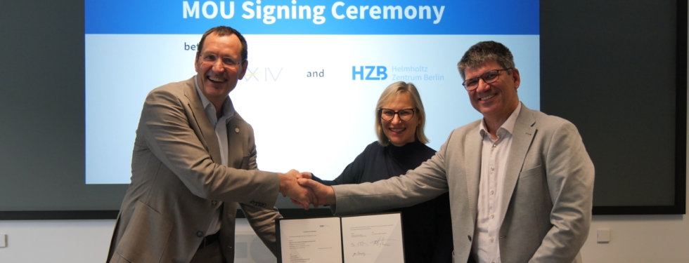
Swedish national synchrotron laboratory MAX IV and Helmholtz-Zentrum Berlin (HZB) BESSY II light source announce the signing of a 5-year cooperation agreement. The new agreement establishes a framework to strengthen cooperation for operational and technological development in the highlighted fields of accelerator research and development, beamlines and optics, endstations and sample environments as well as digitalisation and data science.
